Optical Defect Inspektion

• Optical inspection for marco defects and micro defects

• Visual information of defects and their mapping

• Systems with manual wafer handling and automatic mapping function

• Bare and pattern samples

• Wafer on dicing tapes

• Dies in Waffle packs

nSpec LS defect inspection

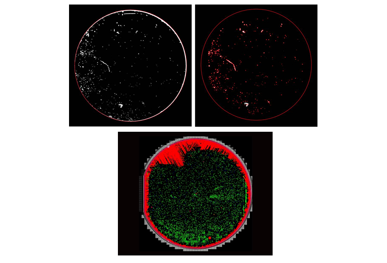
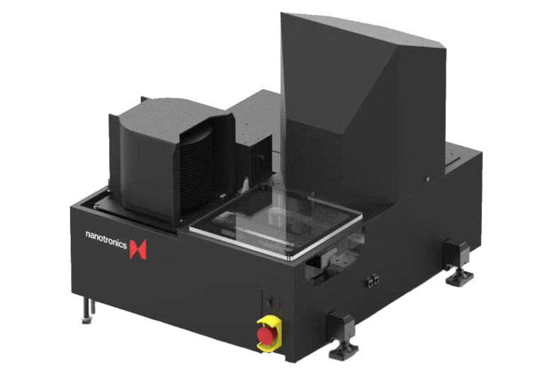
• Semi-automatic defect inspection system

• Defect inspection for:
    Substrate wafer / EPI wafer / patterned wafer / Diced wafer / Dies and Individual samples

• Create different receipt with rapid scanning, mosaicking user-specific way for presenting results, defect classification

• Save image data for records or additional image processing with different parameter settings

• Result data communication with different communication formats, e.g. KLARF

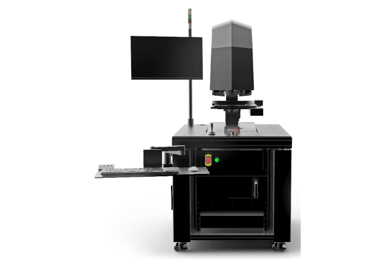
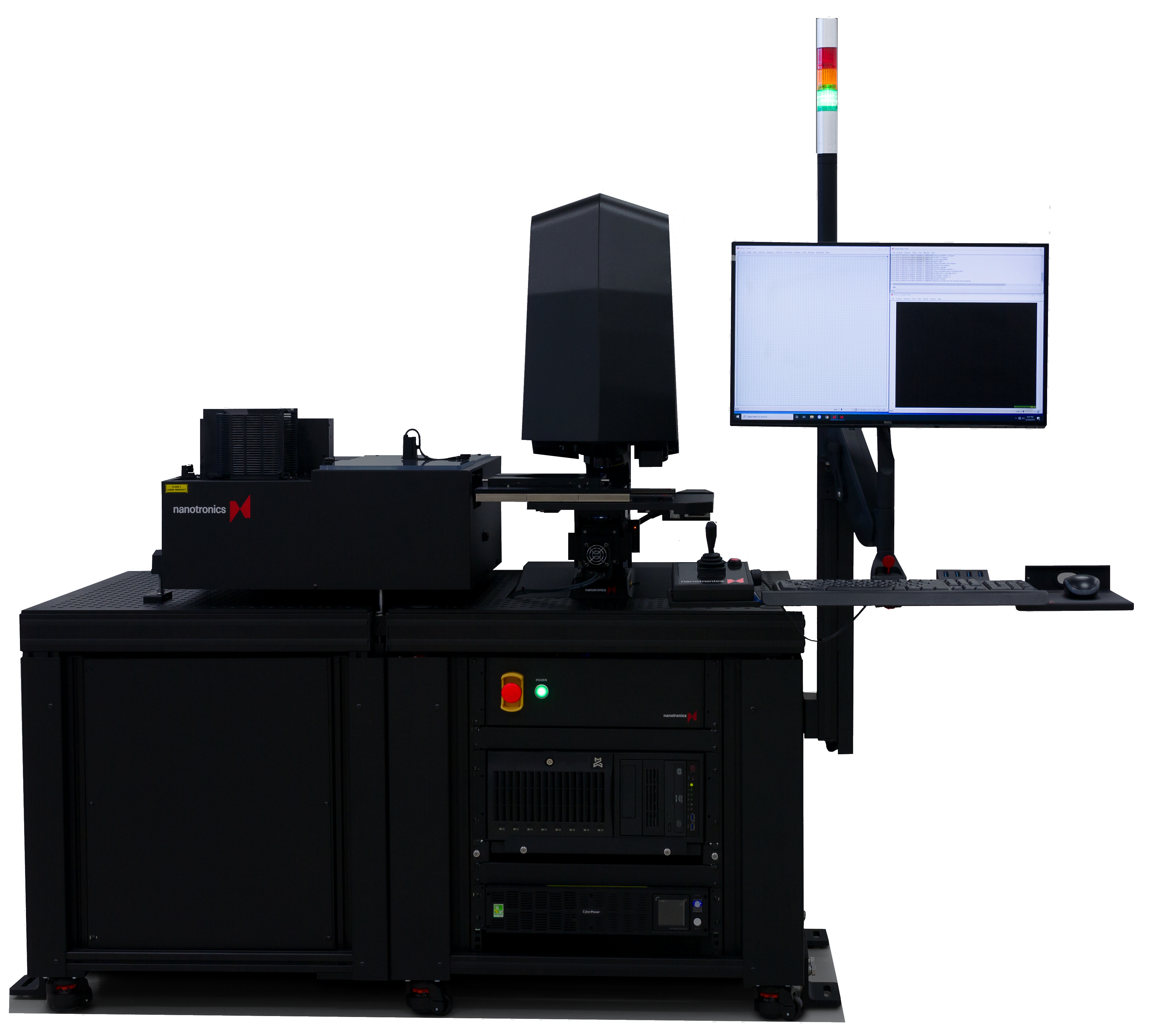
• High resolution microscope with object lenses from 2,5x to 50x

• LED lightning for BF;DF and DIC, transmitted light option

• Motorized X/Y-Stage with 0.04µm increment

• Wafer chuck for 2”,3”, 100mm, 150mm and 20mm or other sample holder available

nSpec PS defect inspection

• Automatic defect inspection

• Defect inspection for: Substrate wafer / EPI wafer / patterned wafer / Diced wafer / Dies Individual samples

• Create different receipt with rapid scanning, mosaicking user-specific way for presenting results, defect classification

• Save data as e.g. KLARF or CSV

• High resolution microscope with objective from 2,5x to 50x

• LED lightning for BF;DF and DIC, transmitted light option

• Motorized X/Y-Stage with 0.04µm increment

• Wafer chuck for 2”,3”, 100mm, 150mm and 20mm or other sample holder

• Wafer loader with pre-aligner

• Carrier and wafer size detection

• OCR reader option

• GEM/SECS Option

nSpec PS-300 defect inspection

• Automatic defect inspection

• Defect inspection for: Substrate wafer / EPI wafer / patterned wafer / Diced wafer / Dies Individual samples

• Create different receipt with rapid scanning, mosaicking user-specific way for presenting results, defect classification

• Save data as e.g. KLARF or CSV

• High resolution microscope with objective from 2,5x to 50x

• LED lightning for BF;DF and DIC, transmitted light option

• Motorized X/Y-Stage with 0.04µm increment

• Wafer chuck for 100mm, 150mm , 200mm, 300mm

• Wafer loader with pre-aligner

• Carrier and wafer size detection

• OCR reader option

• GEM/SECS option

nPlace Marco Defect Inspections

• Automatic macro defect inspection system for wafer size from 2” to 200mm

• Inspection of the whole wafer surface

• Recipe configuration with different light sources in angle or color

• Single shot picture of the entire wafer surface

• Defect analyze with classification of defects

• Resolution of defects, scratch and other artefact >75µm

• Result data communication with different communication formats, e.g. KLARF

• Automatic wafer carrier detection and parameter control

• Automatic wafer loader for wafer sizes from 2” up to 200mm